Over the past several years, Intel has faced stalled technology advances, critical decision-making missteps, and mounting pressure from competitors. Once the undisputed leader in semiconductor manufacturing, the company rapidly lost its process advantage. Intel not only missed the pivotal window created by the explosive growth in AI computing demand, but also saw widening financial losses and continued erosion of market share—at one point even confronting serious questions around potential breakups and long-term corporate viability.
However, following Intel’s showcase of the Panther Lake processor at CES and the disclosure of the latest progress on its 18A process, the company has begun to demonstrate tangible breakthroughs across advanced manufacturing and product roadmaps. Whether 18A can become the key inflection point that brings Intel back to the center of industry competition and rebuilds its long-term competitiveness has now become a major focus for the market.
Introduction to the 18A Process
Process Positioning and Strategic Significance
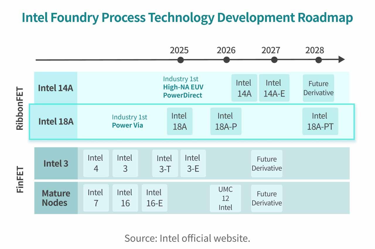
Intel 18A plays a pivotal role in Intel’s process roadmap and represents a core milestone in its effort to reclaim leadership in advanced manufacturing. Through 18A, Intel aims not only to rebuild process advantages for its own product portfolio, but also to position the node as the flagship offering of Intel Foundry Services (IFS), directly targeting TSMC’s leadership in the advanced-node market.
The 18A process introduces several key technology innovations, including the PowerVia backside power delivery architecture and RibbonFET (GAA) transistor design. These are expected to deliver meaningful improvements across PPA metrics—performance, power efficiency, and area. According to Intel’s plans, 18A will be among the earliest sub-2nm-class nodes in North America capable of volume production. For customers seeking to diversify supply-chain risk and manufacture advanced chips on US soil, this provides significant strategic appeal.
18A Technical Details
RibbonFET (Gate-All-Around Transistors)
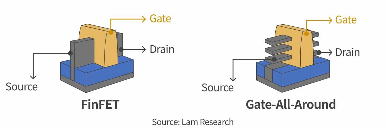
As chips continue to scale down, FinFET transistors have reached physical limits, with increasing leakage and diminishing scaling benefits. Gate-All-Around (GAA) transistors such as RibbonFET are widely viewed as essential to extending Moore’s Law. This marks a major shift for the semiconductor industry, replacing the FinFET architecture that has dominated for over a decade and enabling scaling toward 2nm and beyond.
Conceptually, GAA transistors transform the conduction channel from a vertical “fin” into horizontally stacked “ribbons,” with the gate fully surrounding each channel. This structure delivers superior electrostatic control, which is especially critical for future AI computing and high-performance data centers. While this transistor class is broadly referred to as GAA, naming differs by company: Intel calls its implementation RibbonFET, Samsung uses MBCFET (Multi-Bridge Channel FET)—already in volume production at 3nm—while TSMC generally refers to its design as GAAFET.
PowerVia (BSPDN Backside Power Delivery)
In conventional front-side power delivery designs, power and signal lines are densely intertwined, leading to severe metal congestion, rising resistance, and voltage droop—ultimately constraining performance and energy efficiency. To address these issues, Intel introduced the industry’s first PowerVia backside power delivery network (BSPDN), which has become one of the defining technologies of the 18A generation.
PowerVia relocates the entire power delivery network from the front side of the chip to the backside, using nano-scale through-silicon vias (Nano-TSVs) within standard cells to supply power more directly and with lower resistance. By fully separating power and signal routing, PowerVia frees up front-side metal layers, eases routing congestion, improves design flexibility, and significantly reduces voltage droop.
From a performance standpoint, PowerVia can increase standard-cell utilization by approximately 5% to 10% and deliver up to a 4% improvement in ISO power efficiency. In addition, front-end metal RC performance improves by roughly 12%, while via resistance can be reduced by as much as 49%, resulting in substantially better power integrity. Intel 18A offers both a 180CH high-performance library and a 160CH high-density library to support diverse application needs. Intel’s early move to validate PowerVia on Intel 3 test chips has also improved the maturity and readiness of this technology for 18A volume production.
Lithography Technology
A key success factor for Intel 18A lies in its early deployment of High-NA EUV (high numerical aperture extreme ultraviolet) lithography tools. As one of ASML’s first customers for this equipment, Intel accumulated critical exposure parameters and design rules during the 18A R&D phase, laying the physical foundation for its future 14A leadership.
While early 18A volume production will adopt a flexible approach—combining standard 0.33 NA EUV multiple patterning with selective use of High-NA tools to balance capacity and cost—Intel’s early mastery of High-NA EUV provides longer operational experience and richer technical data than peers. This advantage is decisive for achieving finer patterning and reducing overall process steps at nodes below 2nm.
Omni MIM Capacitor Applications (Not Exclusive to 18A)
In high-performance computing, transient power droop remains a major challenge for voltage stability. To address this, Intel has introduced next-generation high-density metal–insulator–metal (MIM) capacitors into the 18A process. These miniature capacitors are widely distributed across circuit layers, serving as localized energy storage and balancing elements that provide immediate buffering during sudden current spikes.
By significantly mitigating power fluctuations, these capacitors enhance operational stability under heavy workloads. This relentless focus on power integrity is fundamental to ensuring reliable operation at 2nm-class precision, delivering clean and stable power to transistors. For modern workloads such as generative AI—characterized by highly bursty compute demand—precise, real-time power buffering is essential to maintain uninterrupted system performance.
Advanced Packaging and 3D Stacking: Foveros (Not Exclusive to 18A)
Advanced packaging has become a key enabler for extending Moore’s Law and boosting computing performance. Intel’s Foveros 3D packaging technology vertically stacks multiple chiplets with different functions into a single system-on-chip (SoC), dramatically enhancing design flexibility and scalability.
When combined with PowerVia and EMIB, Foveros forms a highly integrated heterogeneous packaging platform, allowing chips to deliver greater compute density and bandwidth within a limited footprint. It is worth noting that TSMC and Samsung have also introduced their own 3D packaging solutions. As such, while Foveros remains a core Intel capability, it does not constitute an exclusive or insurmountable advantage over competitors.
18A Process Applications
The real-world value of 18A will begin to materialize in the first half of 2026 with the launch of Clearwater Forest (Xeon 6+ processors). Featuring 288 efficiency cores and leveraging both PowerVia and Foveros for extreme heterogeneous integration, Clearwater Forest is expected to deliver a 17% IPC improvement over its predecessor.
On the consumer side, Panther Lake processors will validate 18A’s energy efficiency in mobile platforms. These products not only represent a revival of Intel’s internal roadmap, but also serve as flagship proof points for foundry customers, demonstrating Intel’s ability to achieve stable sub-2nm-class production within the United States.
Competitive Landscape: Roadmaps of Other Foundries
Beyond Intel’s advances, both TSMC and Samsung have made tangible progress at the 2nm node, with both companies entering volume production in 2025. This underscores an industry-wide, multi-front race characterized by dense node transitions and parallel development paths.
TSMC
TSMC’s N2 process is scheduled to enter volume production in 3Q25, followed by a broader N2 family targeting applications across consumer electronics, enterprise computing, and AI. N2 is primarily aimed at mobile devices and wearables, while N2P further optimizes performance and power efficiency for flagship smartphones and high-performance laptops. The A16 node is expected to integrate more advanced packaging technologies, focusing on scalable architectures for high-performance computing and cloud AI.
| Performance | Power | Density | Volume Production | Applications | |
|---|---|---|---|---|---|
| N2 (vs N3E) | +10–15% | −25–30% | +15% | 3Q25 | Mobile |
| N2P (vs N2) | +5–10% | −5–10% | Same as N2 | 2H26 | Smartphones |
| N2X (vs N2) | +5–10% | – | – | 2027 | – |
| A16 (vs N2P) | +8–10% | −15–20% | +7–10% | 2H26 | HPC |
Samsung
Samsung’s 2nm process, branded SF2, enters volume production in 2025, initially focused on mobile processors, with its first product being the in-house Exynos 2600. In 2026, Samsung plans to roll out SF2P, delivering roughly 12% performance gains and 25% power reduction versus the prior generation. Market rumors suggest Tesla’s AI6 chip may adopt SF2P. Samsung is also planning SF2X for HPC and AI workloads, while SF2A targets automotive applications with mass production expected in 2027.
Comparison of Intel, TSMC, and Samsung at 2nm
| Intel | TSMC | Samsung | |
|---|---|---|---|
| Process Name | 18A | N2 | SF2 |
| GAA Architecture | RibbonFET | Nanosheet | MBCFET |
| Backside Power | Yes (PowerVia) | A16 (Super Power Rail) | 2027 (PowerVia-like) |
| Performance | +25% (vs Intel 3) | +10–15% (vs N3E) | +5% (vs SF3) |
| Power | −36% (vs Intel 3) | −25–30% (vs N3E) | −25% (vs SF3) |
| Yield | 50% | ~90% | 50% |
| Volume Production | 2H25 | 3Q25 | 2025 |
| Strategic Focus | Major tech leap, reclaim leadership | Stable roadmap, yield and customers | Improve yield, expand customer base |
| Strengths | First mover in backside power | High maturity, strong ecosystem | Early GAA adoption, cost potential |
| Key Challenges | PowerVia integration and yield | – | Yield ramp, competitive pressure |
| Key Customers | Panther Lake (in-house) | MediaTek, Qualcomm, Apple | Exynos 2600 (in-house) |
Intel 18A differentiates itself through the combination of RibbonFET and PowerVia backside power delivery, delivering roughly 25% performance gains and 36% power reduction versus Intel 3. However, Samsung’s SF2 entered volume production earlier in 2025, and TSMC’s N2 followed in 3Q25—both ahead of Intel’s 2H25 timeline.
Notably, TSMC’s N2 leads 18A in both yield and overall maturity, supported by a robust ecosystem and strong customer adoption. Samsung, while benefiting from earlier GAA experience and cost-focused positioning, continues to face challenges in yield ramp and intense market competition. Ultimately, the success of Intel 18A hinges on PowerVia’s mass-production integration and the speed of yield improvement.
Market View and Outlook
The 18A process is a cornerstone of Intel’s foundry ambitions and a focal point for market attention. In recent years, Intel has faced significant competitive pressure in the PC CPU market, largely because AMD leveraged TSMC’s advanced nodes to widen gaps in performance and power efficiency. With its own process roadmap lagging, Intel’s mainstream Raptor Lake remained on a 10nm-class node, limiting competitiveness and forcing a strategic shift toward TSMC manufacturing for Lunar Lake and Arrow Lake.
Panther Lake marks a critical strategic turning point. As the first high-volume product built on Intel 18A, it represents a substantial leap forward, with Intel citing around 60% performance gains versus Lunar Lake and approximately 77% improvement in gaming performance.
For Intel, Panther Lake is not just a generational update—it is central to the long-term sustainability of its foundry business. Production stability and power efficiency will directly influence customer adoption decisions, with designers such as MediaTek and Qualcomm closely watching real-world results. Market speculation also suggests Broadcom may allocate part of its ASIC demand to Intel 18A-P, while Apple is reportedly evaluating a performance-optimized 18A-P for future M-series chips around 2027. If Panther Lake successfully validates maturity and efficiency, Intel’s chances of winning tier-one customers will rise meaningfully. Against the backdrop of structurally tight advanced-node capacity at TSMC, 18A—and later 14A—carry meaningful strategic optionality.
Conclusion: A Defining Moment for Technology and Execution
Intel 18A represents more than a process node—it is a critical test of Intel’s technology strategy, foundry ambitions, and long-term competitiveness. Through the simultaneous adoption of RibbonFET and PowerVia, Intel has achieved a generational shift in both transistor architecture and power delivery, restoring its ability to compete head-on with TSMC and Samsung in the sub-2nm era.
That said, industry reality shows that TSMC’s N2 has entered production with higher yields and a more mature ecosystem, while Samsung has secured early positions in mobile and targeted application markets. Advanced-node competition has increasingly become a contest of execution quality and customer trust.
For Intel, the production performance of Panther Lake and Clearwater Forest will determine whether 18A evolves beyond a technology showcase into a scalable foundry node. If Intel can successfully validate yield, energy efficiency, and delivery stability, 18A—and subsequently 14A—could emerge as viable alternatives for leading customers amid persistent capacity constraints at TSMC. If not, Intel’s window to close the gap in advanced manufacturing will continue to narrow. Ultimately, the success or failure of 18A will influence not only Intel’s future, but also whether the global advanced semiconductor supply landscape can truly become more diversified.
