As AI and HPC chips continue to evolve rapidly, advanced packaging is increasingly becoming a critical enabler for sustaining computing performance and system-level integration. The inherent limitations of traditional round wafers—particularly in terms of area utilization and packaging efficiency—are becoming more pronounced. As a result, panel-level packaging substrates are widely viewed as an important future direction.
However, as package sizes and the scale of chips and IC substrates continue to grow, traditional ABF substrates are facing increasingly severe challenges related to warpage and structural stability. Against this industry backdrop, TSMC has achieved notable success in the high-performance computing market with its CoWoS packaging technology. Building on this foundation, TSMC is now extending beyond wafers to panels, developing the new CoPoS packaging architecture to address the heightened requirements for yield control and structural reliability posed by large-scale, highly integrated packages.
CoPoS Development Background: Growth Bottlenecks for CoWoS Technology
TSMC’s CoWoS packaging technology has achieved decisive success in the AI chip segment, securing more than 90% market share in the HPC market, with capacity remaining in a prolonged state of undersupply. However, as AI chip sizes continue to expand, CoWoS is gradually encountering unavoidable physical limits, mainly reflected in two areas:
- Declining area utilization of round wafers: Cutting large square dies from 12-inch wafers results in substantial edge waste, rapidly degrading output efficiency. Taking NVIDIA as an example, its B200 chip can place only 16 dies on a 12-inch wafer, compared with 29 dies for H100, highlighting the structural mismatch between expanding die sizes and existing wafer capacity.
- Simultaneous scaling of package and substrate size exacerbates warpage issues: As IC substrate dimensions increase from around 70 mm to nearly 100 mm, traditional ABF substrates face severe challenges in flatness and structural stability. This, in turn, constrains further line width and spacing scaling, making high-density interconnects a key bottleneck for the next stage of advanced packaging.
In this context, while CoWoS remains highly competitive, its growth ceiling is becoming increasingly visible as physical and process limitations emerge—prompting TSMC to actively plan and invest in the next generation of packaging solutions.
Introduction to CoPoS Technology
A Panel-Level Packaging Extension of CoWoS

CoPoS, short for Chip-on-Panel-on-Substrate, can be viewed as an evolution of CoWoS toward panel-level packaging. Its core concept is to replace traditional round silicon interposers with rectangular panels, dramatically improving packaging area utilization by “turning circles into squares.” Importantly, CoPoS does not eliminate silicon interposers. Instead, it uses square materials such as glass or sapphire as temporary carriers, on which RDL (redistribution layers) are fabricated before proceeding with subsequent packaging steps. This architecture is better suited to large package sizes.
Thanks to the ability of square panels to support larger reticle stitching, CoPoS effectively aligns with the ongoing trend of increasing AI chip dimensions.
Breaking Area and Warpage Limits with Square Glass Panels
The core advantage of CoPoS panel-level packaging lies in its significant improvement in area utilization and throughput per unit time, effectively reducing edge waste and material loss, and thereby lowering overall packaging costs. Compared with a mainstream 12-inch (300 mm) round wafer, a square glass carrier with side length of around 310 mm can deliver approximately 1.5× higher effective output under similar process conditions—highlighting the structural advantages of panel-based architectures in cost efficiency and scalable mass production.
In addition, the use of glass substrates brings several key benefits. First, glass offers extremely high flatness, which is critical for lithography and supports finer line width and spacing designs. Compared with ABF substrates that require multiple buildup layers to achieve high-density interconnects, glass carriers are structurally more efficient. Second, glass has a relatively low coefficient of thermal expansion (CTE), around 3–9 ppm/°C, enabling controlled deformation under high-temperature processes and improving process stability and yield.
Glass also provides superior mechanical strength compared with traditional composite materials. Although its brittleness still presents manufacturing challenges, overall it delivers clear advantages in thermal management and warpage suppression. As such, CoPoS is positioned as a key technological pathway for overcoming the physical limits of advanced packaging and supporting large-scale, highly integrated package designs.
| Substrate Material | Silicon | Glass |
|---|---|---|
| Surface flatness | <10 | < |
| CTE (ppm/°C) | 2.9–4 | 3–9 |
| Moisture absorption | 0 | 0 |
| Thermal conductivity (k) | 14,800% | 110% |
| Package size | 35×35 | 100×100 |
Table 1: Glass features a low coefficient of thermal expansion Source: Cathay Securities
CoPoS Progress Update: Mass Production Targeted for Late 2028
Market sources indicate that TSMC plans to establish its first CoPoS pilot line at TSMC Specialty Materials (TSMC subsidiary) as early as 2026, with large-scale mass production targeted at the Chiayi AP7 site by the end of 2028. The timeline could potentially be pulled in, with NVIDIA expected to be the first customer.
On the international front, TSMC is also advancing overseas capacity planning. One building at its planned advanced packaging facility in Arizona—construction expected to begin in 2028—will reportedly be dedicated to CoPoS. In addition, TSMC has recently consolidated a 6-inch fab and three 8-inch fabs in the Hsinchu Science Park, and is evaluating the conversion of some existing sites into advanced packaging facilities. These moves underscore that CoPoS has become a central pillar of TSMC’s mid- to long-term advanced packaging strategy, with a clear increase in resource allocation and strategic priority.
Technology Comparison: CoPoS, CoWoS, and CoWoP
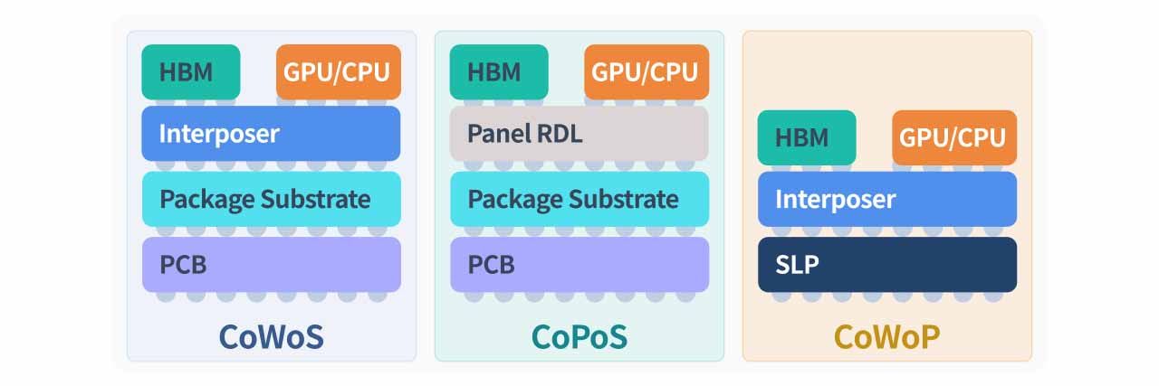
| Technology | CoWoS(Chip-on-Wafer-on-Substrate) | CoPoS(Chip-on-Panel-on-Substrate) | CoWoP(Chip-on-Wafer-on-PCB) |
|---|---|---|---|
| Core concept | Chips integrated with silicon interposer, then mounted on ABF substrate | Chip modules first packaged on panel-level substrate | No ABF substrate; chips and interposer mounted directly on PCB |
| Carrier | 300 mm round wafer | 310×310 mm square glass | – |
| Cost | Highest, due to complex silicon interposer process | Medium; competitive if yields improve | Lowest, potential to reduce CPO manufacturing cost |
| Thermal performance | Requires external thermal solutions | Requires external thermal solutions | Simpler path, large PCB area may aid heat dissipation |
| Strengths | Most mature; supports HBM stacking and high-speed I/O | Highest throughput per unit time; suitable for large dies | Simplified structure, shortest signal path, best theoretical cost |
| Mass production | In production | End-2028 | Timeline unclear |
Overall, CoPoS can be seen as a panel-level extension of CoWoS. By first packaging chip modules on panel-level substrates before backend integration, it replaces CoWoS’s 300 mm round wafer with a 310×310 mm square glass panel. The core value lies in substantially improving area utilization and throughput, making it particularly well suited to the continued expansion of AI chip sizes.
From a cost perspective, CoPoS is currently positioned between CoWoS and CoWoP. As yields and process stability improve, it has the potential to become increasingly cost-competitive. Thermal design requirements remain similar to CoWoS, typically requiring additional cooling solutions. CoWoS, meanwhile, remains the most mature and widely deployed technology, with strong support for HBM and high-speed interconnects, albeit at higher cost due to interposer complexity. CoWoP, characterized by the elimination of ABF substrates, offers a simplified structure, shorter signal paths, and improved thermal flexibility via large PCBs—suggesting the lowest theoretical cost, though its mass production timeline remains uncertain.
Taken together, CoPoS is strategically positioned to balance the high-density interconnect requirements of advanced packaging with improved capacity efficiency and cost structure through panelization, with late 2028 serving as a key milestone for commercialization.
CoPoS-Related Supply Chain
CoPoS Drives Rapid Growth in Panel-Level Packaging Equipment
The panel-level packaging equipment market carries substantial growth potential. Industry estimates suggest that a single CoPoS production line requires equipment investment of approximately NT$10–15 billion. If TSMC builds 5–8 lines as planned, total equipment demand could reach NT$80–120 billion. Factoring in additional demand from advanced packaging facilities in the US, the global CoPoS equipment market could exceed NT$200 billion, presenting significant mid- to long-term opportunities for equipment suppliers.
As the CoPoS mass production timeline becomes clearer, TSMC has gradually released equipment specifications and potential order volumes. An initial group of 26 suppliers—13 from Taiwan and 13 international—has already been shortlisted, signaling both high technical barriers and intensifying competition across the global equipment supply chain.
| Taiwan Suppliers | International Suppliers |
|---|---|
| Gudeng Precision (3680.TW) | KLA Corporation (KLAC.US) |
| Gallant Micro (6640.TW) | Tokyo Electron (8035.T) |
| Grand Process Technology (3131.TW) | Screen Holdings (7735.T) |
| Scientech Corp. (3583.TW) | Applied Materials (AMAT.US) |
| C Sun Mfg (2467.TW) | Disco Corporation (6146.T) |
| APT (7734.TW) | Yamada Corporation (9831.T) |
| Favite, Inc. (3535.TW) | Tazmo (6266.T) |
| Ta Liang Technology (3167.TW) | Nitto Denko (6988.T) |
| Chroma (2360.TW) | Canon (7751.T) |
| V5 Technologies (7822.TW) | LINTEC (7966.T) |
| Semtek (Private) | Camtek (CAMT.US) |
| Manz (Private) | Heller (Private) |
| Leading Precision Inc. (Private) | Nordson (NDSN.US) |
Taiwan Spotlight Companies
Manz (Private)
Manz is one of the few Taiwanese suppliers with core system integration capabilities for panel-level packaging equipment. Leveraging years of experience in RDL process and equipment development, the company has established a semiconductor R&D center in Taoyuan and completed a CoPoS RDL equipment platform capable of both pilot testing and volume production.
Manz’s growth momentum is expected to be driven primarily by rising equipment demand as CoPoS moves toward mass production. RDL is an indispensable core process in CoPoS, directly determining high-density interconnect capability by redistributing chip I/O, shortening signal paths, and improving high-speed, high-frequency transmission performance and stability. As CoPoS lines expand and specifications advance, demand for advanced RDL equipment is set to increase accordingly—positioning Manz as a direct beneficiary thanks to its panel-level RDL and turnkey line solutions.
Overall, Manz has secured a strong position in the CoPoS panelization trend through its “panel-level RDL equipment + turnkey line systems” strategy. With coverage from 300 mm to 700 mm formats, broad process compatibility, and strengths in automation and software integration, the company is well aligned with the structural shift in advanced packaging from wafers to panels and from standalone tools to integrated production lines—offering clear growth visibility as CoPoS capacity scales and interconnect density requirements rise.
APT (7734.TW)
APT (7734.TW) is Taiwan’s first equipment maker to mass-produce high-voltage, high-temperature oven solutions, and is among the most active globally in patent deployment within this field. The company’s core products focus on front-end advanced packaging equipment, with debonding and void-removal systems accounting for around 80% of revenue and commanding roughly 90% market share in advanced packaging debubbling processes. It has also expanded into warpage control, soldering/reflow, and thermal management equipment, offering six major advanced packaging solutions addressing issues such as process-induced bubbles.
Looking ahead to 2026, APT’s growth drivers are expected to come from three main areas:
- Capacity build-outs for CoWoS-L, FOCoS, and CoPoS: The company’s second-generation VTS systems—used for underfill debubbling in CoWoS processes—are expected to see stronger shipments as capacity ramps.
- Warpage control solutions: As advanced packaging moves toward larger formats, warpage has become a critical bottleneck. Innergy’s WSAS systems address warpage, annealing, and thermo-compression annealing needs, and are being promoted as bundled VTS + WSAS solutions across wafer fabs and OSATs for CoWoS, FOCoS, and CoPoS.
- Ramp-up of high-end new tools and thermal materials trends: The fourth-generation RTS targets post-chiplet packaging debubbling and residue removal, significantly shortening process time at bake and clean steps while improving throughput. The third-generation Pioneer & PRO systems support high-temperature vacuum press environments and reflow or dielectric material baking, and are suitable for future metal thermal interface materials—representing non-substitutable new equipment demand that should lift ASPs and margin structure.
Overall, APT has established strong customer stickiness and market leadership through its front-end advanced packaging debubbling equipment. By expanding into warpage control, cleanliness, and process stability solutions required by large-format panel-level packaging, the company is well positioned to directly benefit from CoPoS capacity expansion.
