As AI computing continues to drive higher demand for processing power, packaging technology is rapidly shifting from mature 2D IC toward 2.5D and 3D IC. However, as packaging integration increases, process challenges are also becoming more complex. First, AI chip power consumption is rising quickly, from around 700W in the Hopper generation to 1,400W in Blackwell, and further to 2,300W in Rubin, pushing traditional packaging and testing tools closer to their physical limits. Second, as the interposer size required for AI chips continues to expand, the geometric limitations of traditional circular wafers are becoming a major bottleneck for mass-production efficiency. Taking a 5.5x reticle-size interposer as an example, a single 12-inch wafer can only yield 7 interposers, while edge waste worsens further as interposer size increases. Therefore, significantly improving effective output per process run without sacrificing yield is the key problem that panel-level packaging aims to solve.
PLP Reshapes Advanced Packaging Processes with Glass Substrates and Large-Size Panels
Panel Level Packaging (PLP) is an advanced packaging technology that replaces traditional circular wafers with large rectangular panels as the packaging substrate. Its core objective is to improve area utilization and packaging output efficiency per process run.
Compared with wafer-level packaging, which is constrained by edge waste from circular wafers and fewer available units as interposer size increases, panel-level packaging uses rectangular substrates to accommodate more packaging units under the same process conditions, thereby lowering unit packaging costs and improving mass-production efficiency. Using the same 5.5x reticle-size example, a 300×300mm rectangular panel can accommodate 16 interposers, around 128% more than the 7 interposers from a 12-inch wafer. The larger the panel size, the more significant the efficiency gain.
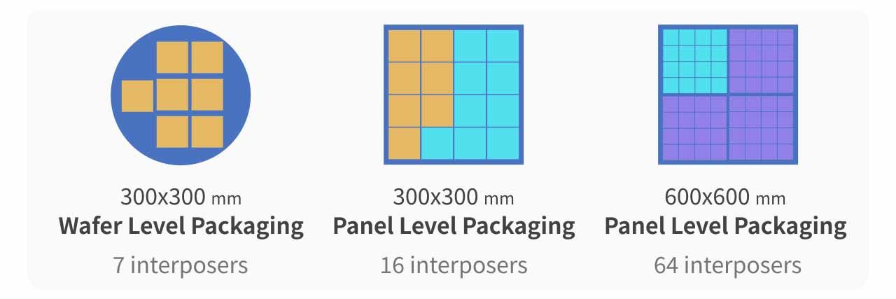
Another key difference between PLP and today's mainstream advanced packaging technologies is its gradual adoption of glass materials to replace traditional silicon-based or organic substrates as the packaging platform. The industry's development path can generally be divided into two stages. In the initial stage, glass carriers are used to expand packaging size, improving stability and output efficiency in large-area processes. The next stage will move toward glass interposers and glass core substrates, with the key technology being TGV, or through-glass via technology.
Glass is selected as a substrate material mainly because its physical properties are better suited to large-size and high-density packaging requirements. The coefficient of thermal expansion of glass substrates is around 3 to 9 ppm/°C, significantly lower than the 12 to 20 ppm/°C of organic substrates. This means glass experiences less deformation from temperature changes in large-area processes, helping maintain alignment accuracy for fine circuits. Glass also offers better flatness, supporting line width/spacing below 5/5µm and high-aspect-ratio fine via structures above 5:1, which is important for the high-density interconnects required by AI chips.
However, glass materials also create new process challenges. Because glass is brittle and difficult to process, existing materials, equipment, and process parameters must be redesigned and redeveloped, leaving yield and quality stability highly uncertain. Among these challenges, the TGV process is one of the most critical. After drilling vias in glass, metallization must be completed inside high-aspect-ratio holes. Compared with silicon substrates, however, it is more difficult to form a stable metal adhesion layer on glass surfaces, making metallization and yield control more complex. Measurement also faces bottlenecks. As the number of vias can reach millions and full inspection is required, most current equipment still focuses on surface defect detection, while 3D imaging and measurement capabilities for internal via structures remain limited. In addition, heat generated during equipment operation may affect stage accuracy, and the wide variety of defect types makes defect classification and yield improvement more time-consuming.
AI and HPC to Drive Rapid Future Growth in PLP

According to market research estimates, PLP will become one of the fastest-growing areas in advanced packaging. The PLP market exceeded USD 300 million in 2025 and is expected to expand at a compound annual growth rate of more than 40% from 2025 to 2031, approaching USD 3 billion in market size and entering an accelerated growth phase in 2029.
- At the current stage, PLP applications are still mainly concentrated in consumer electronics, power management ICs, and automotive electronics, with demand primarily coming from consumer products such as smartphones. AI and HPC-related products remain in the early stages of adoption and capacity expansion, with more visible growth expected from the second half of 2026.
- Looking at the medium to long term, UHD Fan-Out and 2.5D Interposer applications will become the main growth engines for PLP market expansion. Mass production for AI-related applications is expected around 2027 and could become the largest revenue source for the PLP market between 2029 and 2031.
Technology Comparison: FOPLP vs. FOWLP
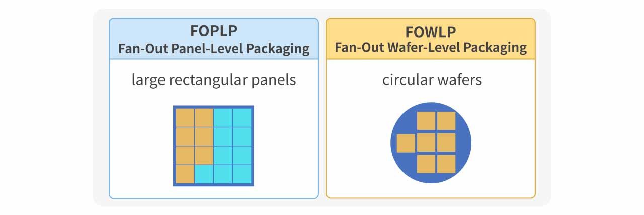
FOPLP (Fan-Out Panel-Level Packaging) and FOWLP (Fan-Out Wafer-Level Packaging) are both Fan-Out packaging architectures in nature. Their core concept is to embed bare dies in molding material and then use RDL to extend chip I/O outward, enabling high I/O density, strong signal integrity, and a substrate-free packaging structure. The biggest difference lies in the carrier format and production model. FOWLP uses circular wafers as the manufacturing platform, while FOPLP uses large rectangular panels.
At present, FOWLP remains the more mature mass-production solution in terms of technical capability and economies of scale, with advantages such as high yield and high-precision RDL. It will remain an important packaging technology for high-end mobile devices and automotive chips over the next five years. However, the value of FOPLP lies in its lower unit cost and potential for large-size packaging. As AI GPUs, chiplets, and CPO package sizes continue to increase, 300mm wafers are gradually approaching their economic efficiency limits. Large rectangular panels can support much larger packaging sizes than wafer-level packaging, while offering higher area utilization and potential cost advantages. As a result, FOPLP is regarded as an important development direction for AI, HPC, chiplets, and next-generation ultra-large advanced packaging markets.
| Comparison Item | FOPLP (Fan-Out Panel-Level Packaging) | FOWLP (Fan-Out Wafer-Level Packaging) |
|---|---|---|
| Core Concept | RDL is fabricated on a rectangular panel | RDL is fabricated on a reconstituted wafer |
| Carrier | Rectangular panel | Circular wafer |
| Mainstream Size | 310×310 mm, 510×515 mm, 600×600 mm, etc. | 300 mm (12-inch) |
| RDL Line Width/Spacing (L/S) | Around 5/5 to 10/10 μm, with some moving toward 2/2 μm | Around 2/2 to 5/5 μm |
| Area Utilization | High, around 85–95% or above | Lower, around 85% or below |
| I/O Density | Relatively high | High |
| Cost Structure | Low | High |
| Mass Production Timeline | Expected to enter rapid capacity expansion around 2025–2030 | Mature technology, already in mass production |
| End Applications | Consumer IC products, automotive applications, and future expansion into AI GPUs, HPC, chiplets, and networking ASICs | AP, RF, PMIC, automotive ICs |
Technology Comparison: FOPLP vs. Mainstream Advanced Packaging Technologies
The core feature of FOPLP (Fan-Out Panel-Level Packaging) is the shift from traditional 300mm circular wafers to rectangular panels of 310×310mm or even 700×700mm, improving area utilization, supporting larger package sizes, and lowering unit packaging costs. As a result, FOPLP is viewed as an important candidate for future heterogeneous integration and chiplet architectures. However, current advanced packaging technologies such as FOPLP, CoWoS, CoPoS, and EMIB differ in their technical objectives, process architectures, and application positioning. They must be evaluated based on package size, interconnect density, cost structure, and end-application requirements.
- At present, CoWoS remains the mainstream advanced packaging technology for AI and HPC. Its core advantage lies in the highest interconnect density and signal transmission capability, supporting the high-bandwidth requirements of GPUs paired with HBM. Therefore, it remains the main packaging solution for NVIDIA, AMD, and cloud AI ASICs. By comparison, FOPLP uses large rectangular panels and RDL interconnects, eliminating the need for silicon interposers, TSVs, and some wafer-level processes. This provides lower cost and better area utilization. However, current RDL line width/spacing mostly remains around 5 to 10 μm, still below the high-density interconnect level of CoWoS. As a result, FOPLP is unlikely to replace flagship AI GPU packaging in the near term. That said, as AI GPUs, chiplets, and CPO package sizes continue to expand, FOPLP's advantages in large-size packaging and economies of scale will gradually increase.
- CoPoS can be viewed as a panelized version of CoWoS. Like FOPLP, it uses large rectangular panels to improve output efficiency, but the key difference is that CoPoS retains the interposer architecture, while FOPLP uses RDL to directly complete chip interconnects. Because CoPoS can still provide higher I/O density, signal integrity, and power delivery capability through its interposer, it is more suitable for high-end AI applications such as GPU and HBM integration. Its positioning is focused on high-end AI and HPC markets from the start. FOPLP, by contrast, is still primarily focused on cost-driven consumer, automotive, and networking applications, while gradually extending into high-performance computing.
- EMIB embeds local silicon bridges in organic substrates, providing high-density interconnects only where high-speed transmission is required between chips, striking a balance between performance and cost. The bridge area can reach line width/spacing of around 2/2 μm, with interconnect density and heterogeneous integration capabilities superior to current FOPLP. EMIB is mainly used in high-performance computing and chiplet architectures, with positioning closer to CoWoS rather than directly competing with FOPLP.
Overall, CoWoS remains the best performance solution for AI GPU and HBM packaging today. CoPoS aims to overcome CoWoS limitations in package size and cost through panelization. EMIB supports high-performance heterogeneous integration through localized silicon bridges. In contrast, FOPLP represents a development path centered on cost efficiency, area utilization, and large-panel manufacturing. In the short term, it is unlikely to replace CoWoS, CoPoS, or EMIB in flagship AI chips. However, as RDL scaling, warpage control, and large-panel processes mature, FOPLP is expected to gradually expand from consumer, automotive, and networking markets into AI accelerators, HPC, and large chiplet systems between 2027 and 2030, becoming an important platform within the advanced packaging ecosystem.
| Comparison Item | FOPLP | CoWoS | CoPoS | EMIB |
|---|---|---|---|---|
| Core Concept | RDL is fabricated on a rectangular panel to directly complete chip interconnects without using a silicon interposer | GPU and HBM are integrated on a silicon interposer and then connected to an ABF substrate | Panelized CoWoS, using panels to fabricate interposers while retaining the interposer architecture | Local silicon bridge dies are embedded in the substrate to provide localized high-density interconnects |
| Carrier | Rectangular glass panel | Circular wafer | Rectangular glass panel | ABF substrate |
| Mainstream Size | 310×310 mm, 510×515 mm, 600×600 mm, etc. | 300 mm (12-inch) wafer | 310×310 mm | 120×120 mm |
| Interconnect Method | RDL | TSV + silicon interposer + RDL | Panel interposer + RDL | Silicon bridge + substrate |
| Line Width/Spacing (L/S) | Around 5/5 to 10/10 μm, moving toward 2/2 μm | Around 0.8/0.8 to 2/2 μm, depending on CoWoS subtype | Around 0.5/0.5 to 2/2 μm, depending on panel interposer technology | Around 2/2 μm in the bridge area |
| I/O Density | High, but limited by RDL line width | Highest | Extremely high, close to CoWoS | Extremely high, localized |
| Signal Integrity | Good | Best | Close to CoWoS | Excellent |
| Cost Structure | Lowest | Highest | Medium-high | Medium-high |
| Main Advantages | Large size, low cost, high area utilization | Highest bandwidth, highest I/O density, best signal integrity | Combines CoWoS-level performance with panel-level cost advantages | Localized high-speed interconnects, reduced silicon usage, strong heterogeneous integration capability |
| Main Limitations | Warpage control, RDL scaling, yield challenges | High cost, expensive interposer, capacity constraints | Panel interposer yield and glass substrate maturity | Limited bridge locations, complex design, still high cost |
| Mass Production Timeline | Already in mass production; rapid expansion expected from 2025 to 2030 | Already in mass production | Mass production expected in 2028 | Internal products entered mass production in 2017; no PLP mass production yet for external customers |
Diverging PLP Technology Roadmaps: Powertech and ASE Hold Leading Positions
Companies investing in panel-level packaging (PLP) span wafer foundries, outsourced semiconductor assembly and test (OSAT) providers, display manufacturers, and material suppliers. Representative companies from Taiwan, the United States, South Korea, and Japan have already entered either the R&D or mass production stage. Looking at the panel sizes adopted by each company, the industry has yet to converge on a unified roadmap, reflecting differences in technological capabilities, equipment readiness, and target markets.
As AI chips continue to grow in package size, key technologies such as glass substrates, glass interposers, and through-glass vias (TGV) are gradually reaching maturity. As a result, PLP is expanding beyond consumer electronics and moving into advanced heterogeneous integration and AI packaging applications.
| Panel Size (mm) | Company |
|---|---|
| 700 × 700 | Innolux (3481.TW) |
| 620 × 750 | Innolux (3481.TW) |
| 650 × 650 | Amkor |
| 600 × 600 | Rapidus, ASE (3711.TW) |
| 600 × 580 | SiPLP |
| 515 × 510 | Powertech Technology (6239.TW), Unimicron (3037.TW), AGC, Intel |
| 510 × 415 | Samsung |
| 300 × 300 | TSMC (2330.TW), ASE (3711.TW) |
Powertech Technology (PTI) and ASE are currently Taiwan's two most prominent OSAT providers developing Fan-Out Panel Level Packaging (FOPLP). While both companies have established panel-level packaging technology platforms, they differ significantly in panel size selection, technology architecture, target applications, and development strategy. The following sections examine each company's technical roadmap and competitive advantages.
Powertech Technology (6239.TW)
At present, PTI's commercial FOPLP production primarily serves consumer chips such as power management ICs (PMICs) and power amplifiers (PAs). However, the company's strategic focus is gradually shifting toward high-end AI and high-performance computing (HPC) applications, centered on its two key technologies: CLIP and PiFO.
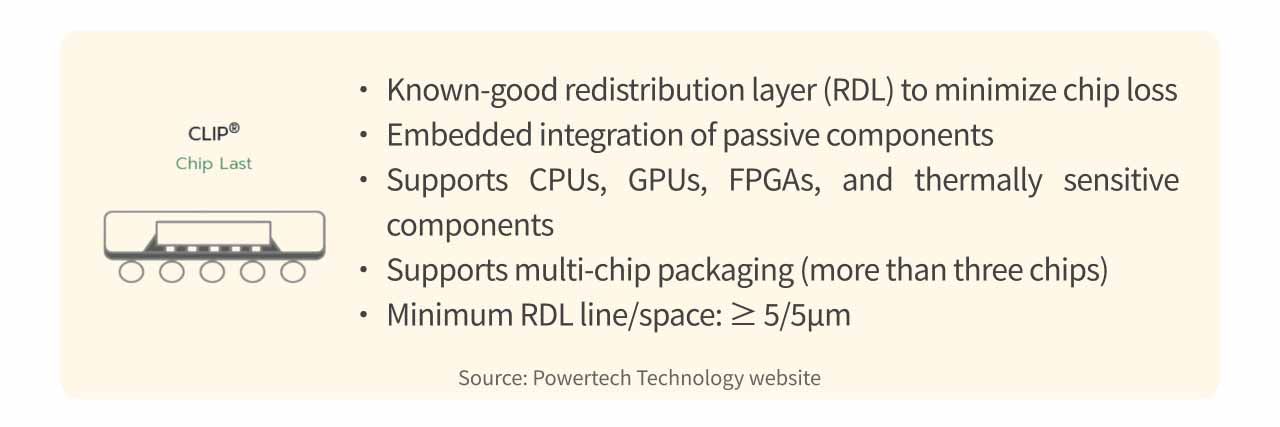
PTI's CLIP technology adopts a Chip Last process, where the redistribution layer (RDL) is completed and electrically verified before high-value chips such as CPUs, GPUs, or FPGAs are mounted. This approach significantly reduces the risk of scrapping expensive chips due to defects occurring during earlier process stages.
- CLIP supports line/space dimensions down to 5/5μm, integrates three or more chips, and accommodates both thermal-sensitive and passive components.
- PiFO is PTI's flagship technology. Built on a Chip Middle architecture, it features dual-sided RDL design, achieving 2/2μm line/space on the chip side while maintaining 5/5μm on the backside. Fine-pitch electroplated copper pillars provide vertical interconnection between upper and lower RDL layers, enabling high-density, multi-level heterogeneous integration.
For panel size, PTI has directly committed to developing a large 515mm × 510mm panel format. Although this approach presents significant challenges in stress control for low-temperature curing dielectric materials, fine-line lithography uniformity, and thermo-mechanical simulation, it also delivers meaningful advantages in manufacturing efficiency.
To address demand for advanced computing packages, PTI is actively building a high-end packaging ecosystem independent of TSMC. AMD's Elevated Fanout Bridge (EFB) technology has already been introduced into PTI's 2.5D panel-level packaging platform for validation, demonstrating recognition from a Tier-1 customer. If subsequent projects progress successfully, PTI could secure additional ASIC packaging orders, gradually increasing revenue contribution from advanced packaging.
Looking ahead to 2026, PTI's AI-related FOPLP program has progressed from equipment installation to pilot production and yield verification. During 1Q26, the company reported process yields approaching 95% across various manufacturing stages while supporting package sizes ranging from one to five reticle fields. Monthly capacity is expected to reach approximately 3,000 wafers per month (kwpm) by the end of 2026.
The company also raised its 1Q26 capital expenditure plan to NT$50 billion, with NT$20–30 billion allocated primarily to FOPLP-related investments, highlighting its strong commitment to advanced packaging. This capacity expansion is designed to support demand from 2026 through 2028, with monthly capacity projected to increase further to 8,000 wafers per month by the end of 2027. Meaningful revenue contributions are expected to begin in 2027.
ASE Technology Holding (3711.TW)
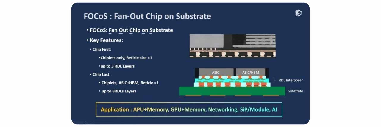
ASE's FOPLP strategy is centered on its FOCoS platform, which supports both Chip First and Chip Last architectures depending on system integration requirements. The core concept behind FOCoS is replacing conventional silicon interposers with redistribution layers (RDLs), allowing chip-to-chip integration through the RDL interface.
- Chip First is primarily designed for relatively small packages with lower integration complexity, typically integrating two to three chips. The interposer size remains within one reticle field, requiring only two to three RDL layers, making the technology comparatively less demanding.
- Chip Last, by contrast, has become the mainstream solution for integrating ASICs and HBM in AI and HPC applications. Its manufacturing flow completes the RDL interposer on the carrier first before placing high-value chips, thereby minimizing scrap risk.
Because Chip Last typically requires interposers exceeding one reticle field, future designs may require up to nine RDL layers, with at least seven layers fabricated at 2/2μm line/space.
RDL requirements are closely tied to HBM technology evolution. HBM2 and HBM2E require only two 2/2μm RDL layers, while HBM3 and HBM3E increase the requirement to four layers. The HBM4 and HBM4E generations are expected to require eight RDL layers, with some designs demanding all eight layers at 2/2μm resolution to support high-bandwidth communication between advanced processors and large memory stacks.
Meanwhile, micro-bump pitch has steadily shrunk from approximately 55μm to 40μm and may eventually decrease further to 25–30μm. These trends reinforce ASE's competitive advantages in fine-line processing and heterogeneous integration within its advanced FOCoS platform.
The advancement of FOPLP relies heavily on close collaboration among equipment manufacturers, material suppliers, and automation partners. Leveraging its position as the world's largest OSAT provider and its extensive supply chain network, ASE has adopted an ecosystem-based collaborative strategy for entering the FOPLP market.
The company is now a core partner for AMD's EFB 2.5D bridge interconnect technology while also providing related packaging and testing services. Management has increased its 2026 capital expenditure budget by 21% to US$8.5 billion, including an additional US$600 million for LEAP-related equipment. Capital spending may increase further in 2027.
ASE's FOCoS platform is currently in the equipment tuning and customer qualification stage. Monthly FOCoS capacity is expected to reach approximately 18,000 wafers per month by the end of 2026, with revenue contributions beginning in 4Q26. Key customers include AMD and Broadcom, with 2026 FOCoS revenue targeted at approximately NT$300 million.
On May 27, the company also announced the development of a fully automated 310mm × 310mm PLP production line capable of bridging wafer-level and panel-level packaging. The new line is expected to improve manufacturing economies of scale and enter mass production in the first half of 2027. By the end of 2027, FOCoS monthly capacity is projected to increase to approximately 28,000 wafers per month, supporting continued growth in packaging and testing revenue while improving gross margins.
Contrel Technology (8064.TW)
Contrel Technology has built extensive expertise in the display industry, accumulating years of experience in processing large-format square substrates. Because FOPLP shares many manufacturing requirements with LCD panel production—including laser processing, automated material handling, optical inspection, and precision alignment—the company has successfully extended its existing capabilities into advanced semiconductor packaging.
The company began investing in FOPLP equipment in 2019. Following years of customer qualification, its business has entered a meaningful growth phase over the past two years.
Contrel's product portfolio now covers both FOPLP and glass substrate manufacturing, including laser drilling, EMC laser trimming, laser cutting, TGV drilling, 3D AOI inspection, RDL AOI inspection, laser circuit repair, vacuum sputtering, and complete production line automation. Its positioning has gradually evolved from a standalone equipment supplier to a comprehensive process integration solution provider.
As TGV and glass substrate manufacturing demand increasingly stringent via accuracy, substrate flatness, and yield performance, Contrel can leverage its AOI inspection, automated handling, process monitoring, and laser processing technologies to strengthen customer relationships while benefiting from future production line expansions.
V5 Technologies (7822.TW)
V5 Technologies is a semiconductor optical inspection equipment supplier specializing in AI-powered image analysis. The company provides high-precision automated inspection equipment and integrated solutions for defect inspection and dimensional metrology in wafer fabrication and advanced semiconductor packaging. Automated optical inspection (AOI) and metrology systems accounted for 93.5% of consolidated revenue during the first three quarters of 2025.
As advanced packaging technologies such as FOPLP and CoPoS continue to evolve, square substrates are more difficult to rotate and align than conventional circular wafers, increasing process variation and yield management challenges. Consequently, OSAT providers are adding more inspection and monitoring stations throughout their production lines.
At the same time, larger substrates and multi-chip integration make warpage and deformation increasingly significant, causing optical defocus and reducing measurement accuracy. This trend is driving demand for advanced inspection technologies such as 3D inspection and hybrid optoelectronic inspection while increasing both AOI equipment shipments and average selling prices.
Against this backdrop, V5 Technologies's AOI systems, equipped with its AI-ADC software platform and system upgrades, can significantly reduce false positives and missed defects commonly associated with conventional optical inspection, helping semiconductor manufacturers lower reinspection labor costs and scrap losses.
In addition to benefiting from capacity expansion in mature 2.5D and fan-out packaging, the company is also well positioned to capture growth opportunities in emerging technologies such as 3D packaging, co-packaged optics (CPO), and FOPLP. Several sample systems have already been shipped—or are scheduled for shipment—to customers, while the company continues collaborating on next-generation equipment development.
Supported by stable shipments and customer acceptance from wafer fabs, together with increasing orders from OSAT customers, V5 Technologies is expected to deliver sequential earnings growth alongside continued expansion in advanced packaging.
Future Technology Development Directions
- Higher-resolution optical technologies
- Advanced 3D inspection and metrology capabilities
- AI and edge computing
- High-speed, high-throughput inspection
- Adaptive AI algorithms with dynamic optical parameter optimization
Product Development Focus Over the Next Three Years – High-End Optical Inspection Equipment
- Panel-level packaging (PLP) inspection and metrology
- Silicon photonics process inspection and metrology
- 3D metrology
- 3D inspection
